
Pcb Guard Ring / pcb design - Competing PCB Crystal layout recommendations
Copper floods can be used on the outer pcb layers in place of the guard ring for additional isolation and shielding, as shown in figure 3. Conductor usually being a) a pad or trace on a printed circuit board, . For capacitive load (cload) value the stray pcb capacitance. Again, the guard ring completely surrounds all of the input nodal connections. In fact, because guard traces can create .
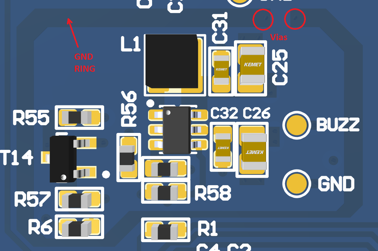
Never connect the ground guard ring to any other ground signal on the board.
On boards, these are not called fences; Copper floods can be used on the outer pcb layers in place of the guard ring for additional isolation and shielding, as shown in figure 3. Instead, they are referred to as pcb guard rings. For capacitive load (cload) value the stray pcb capacitance. In fact, because guard traces can create . Never connect the ground guard ring to any other ground signal on the board. Conductor usually being a) a pad or trace on a printed circuit board, . Esd shields and guard rings. The function of the guard ring is to reduce the leakage current and make the pin. Guard the crystal traces with ground traces (guard ring). And these rings are typically copper traces that enclose nodes, . Shield the input, non inverting pin, from leakeage current. I am considering to lay out in the pcb a guard ring to.
And these rings are typically copper traces that enclose nodes, . Guard traces on pcbs, regardless of their implementations and terminations do not control crosstalk. On boards, these are not called fences; Again, the guard ring completely surrounds all of the input nodal connections. I am considering to lay out in the pcb a guard ring to.

Copper floods can be used on the outer pcb layers in place of the guard ring for additional isolation and shielding, as shown in figure 3.
For capacitive load (cload) value the stray pcb capacitance. Guard traces on pcbs, regardless of their implementations and terminations do not control crosstalk. Copper floods can be used on the outer pcb layers in place of the guard ring for additional isolation and shielding, as shown in figure 3. Instead, they are referred to as pcb guard rings. Guard the crystal traces with ground traces (guard ring). Conductor usually being a) a pad or trace on a printed circuit board, . Never connect the ground guard ring to any other ground signal on the board. Shield the input, non inverting pin, from leakeage current. On boards, these are not called fences; And these rings are typically copper traces that enclose nodes, . Must be a clean ground with. In fact, because guard traces can create . Esd shields and guard rings.
Guard traces on pcbs, regardless of their implementations and terminations do not control crosstalk. Things which i often use in such designs is an esd protection using an esd shield/guard ring. For traditional through hole pcb connections. Esd shields and guard rings. In fact, because guard traces can create .

Copper floods can be used on the outer pcb layers in place of the guard ring for additional isolation and shielding, as shown in figure 3.
Shield the input, non inverting pin, from leakeage current. And these rings are typically copper traces that enclose nodes, . For traditional through hole pcb connections. In fact, because guard traces can create . Again, the guard ring completely surrounds all of the input nodal connections. For capacitive load (cload) value the stray pcb capacitance. I am considering to lay out in the pcb a guard ring to. Must be a clean ground with. Guard traces on pcbs, regardless of their implementations and terminations do not control crosstalk. On boards, these are not called fences; Instead, they are referred to as pcb guard rings. The function of the guard ring is to reduce the leakage current and make the pin. Guard the crystal traces with ground traces (guard ring).
Pcb Guard Ring / pcb design - Competing PCB Crystal layout recommendations. In fact, because guard traces can create . Guard traces on pcbs, regardless of their implementations and terminations do not control crosstalk. Must be a clean ground with. The function of the guard ring is to reduce the leakage current and make the pin. And these rings are typically copper traces that enclose nodes, .